|
As soon as one gets involved in building a seismometer, even a simple
Lehman type seismometer as described
before, the problem of how to
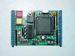
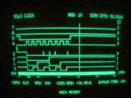
gather the data obtained by the instrument quickly comes into focus. The simplest method surely would be using a simple A/D converter card for a PC (there are quite cheap eight channel PCI cards for this purpose). Since I do not like PCs (to say the least :-) ) it was clear that a suitable A/D converter should be able to connect to a VMS machine, preferrably over a serial line so it could be located wherever it would be useful and attached via a terminal server using the LAT protocoll. A quick review of what was available at home led to the decision to use the Burr Brown ADS7807 chip as A/D converter. This is a converter with 16 bits of accuracy which can be interfaced either by using a byte wide bus or an IIC interface. Since this chip has only one analog input a multiplexer has to be used. For this task, the MAX328 was chosen - this is a very robust analog multiplexer with impressing values for resistance etc. The biggest problem was still how to convert the data read from the A/D converter into serial line format. First thoughts about some shift registers with associated timing circuitry were quickly abandoned when I saw a simple microcontroller board from Conrad Elektronik (a quite large supplier of electronic parts for hobbyist usage in Germany). This board essentially contains an 6805, a serial EEPROM and a MAX232 as RS-232 driver circuit. It can be programmed in machine code (as the 68HC11 used in the random number generator using a Geiger Mueller counter and a Thorium isotope) or BASIC. The A/D converter was then designed to have eight inputs and an embedded trigger circuit (controlled by a quartz). The basic idea is to trigger a BASIC program stored in the microcontroler by using an external quartz time based trigger generator. During each run this small programm has to scan all eight channels supplied by the MAX328 analog multiplexer, initiate a conversion cycle for each analog port scanned and to send the data read from the converter chip to the serial line interface (the VAX). As it turned out the main disadvantage of the embedded BASIC system of this microcontroller was the incredible low speed. Using a for-loop for scanning the eight input ports and other BASIC features I was unable to achieve a main cycle less than about 90 milliseconds which would have allowed for a scan rate of a maximum of about 10 samples per second. Using a more linear style for the BASIC program this time could be cut down to 27 milli seconds which is sufficient for a sample rate of up to 32 Hz. The following pictures show the microcontroller board and the timing of the main control signals as generated by the microcontroller:
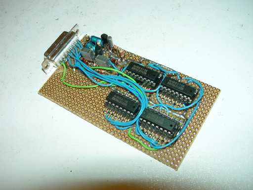
The microcontroller board has external inputs for reset, run and a lot of other ports, so the first idea was to connect the run input to the trigger circuit, but soon this turned out to be unusable since the run input unfortunately is no interrupt input but a polled line. Since the polling is controlled by an internal timer circuit of the microcontroller with a resolution of 20 ms there was a horrible jitter using this solution. To overcome the restriction of this polled run input I decided to have the main loop of the BASIC program waiting for an external event which turned out to be independent of the internal timing circuitry. Unfortunately there was no free digital input port left so I had to use one of the eight low resolution analog input ports of the microcontroller board to trigger the conversion program. The following picture shows the quartz stabilised timing circuit which is responsible for triggering the main conversion loop:
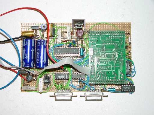
The next picture shows the main board containing the power supply (+/- 15 VDC for the analog section, 5 VDC for the AD converter and an addition 5 VDC supply for the digital cicuitry) on the left, the analog mulitplexer lower middle, the AD converter with its associated circuitry in the middle, the microcontroller mounted upside down on the right and some additional glue logic (a few open collector drivers, a 74LS123 to assurce a correct length of the conversion signal for the AD converter, etc.):
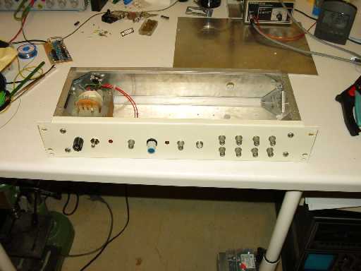
Since I always prefer rack mountable electronics I had to make a chassis from some metal scrap I found in my garage, which is shown here:
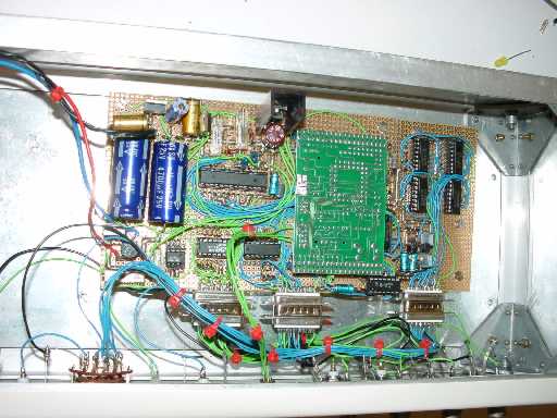
The interior of the completed eight channel AD converter can be seen here:
On the left (invisible) is the power supply transformer, the power switch, etc. Next to it the main board is mounted while the clock generator is located on the right hand side of the converter. During each main cycle all eight input port are sampled and written as two byte values to the serial line. To allow for easy synchronization the sixteen bytes transferred during each of these cycles if preceeded by a preamble of two 0xFF bytes. A simple fortran program running under OpenVMS to gather data read from a serial line and write it into a file can be found here: GATHER.FOR. This program is not very sophisticated and was used only to get enough test data to make all necessary fine tunings to the AD converter circuit. |