|
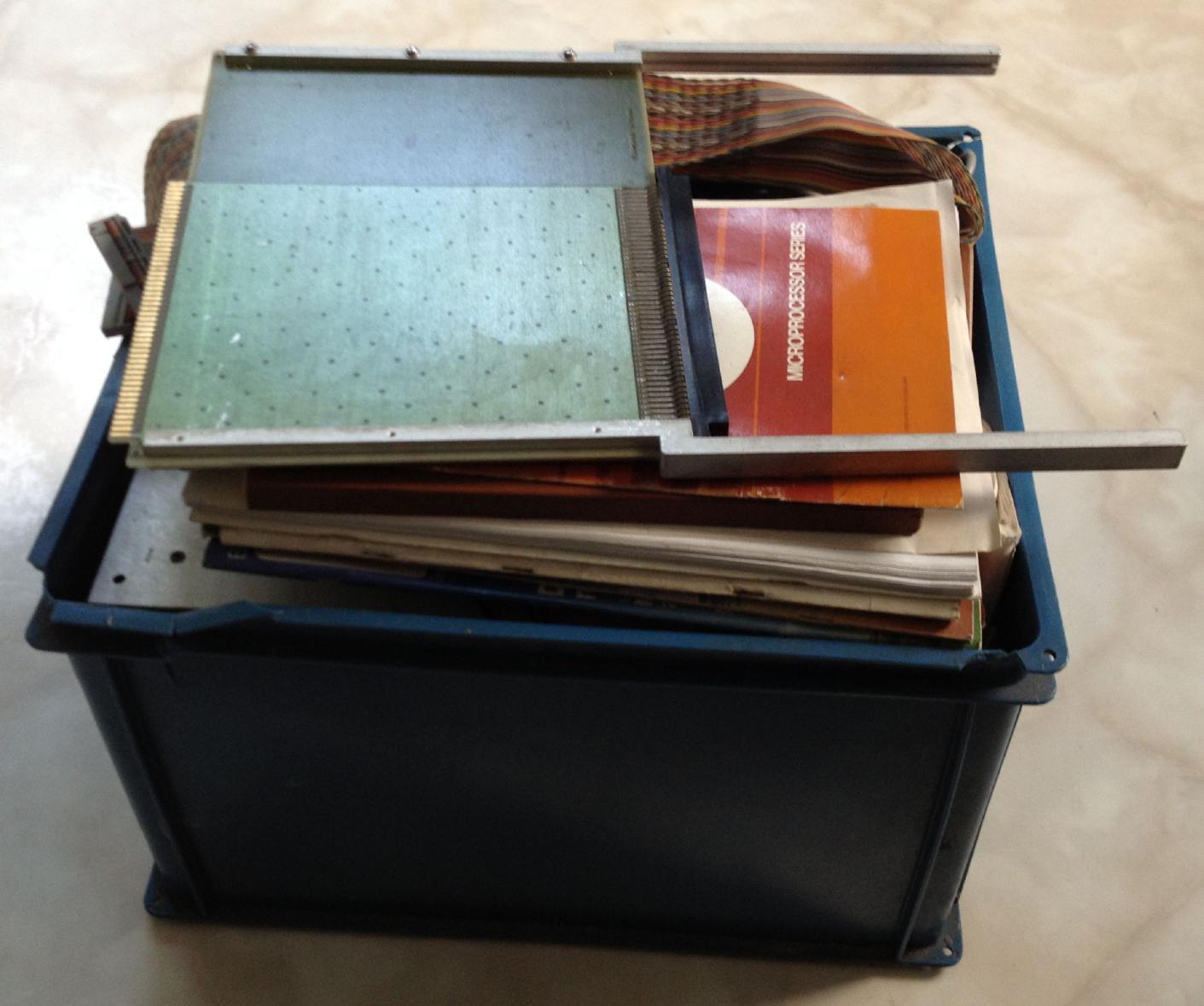
Many years ago, a friend of mine gave me a box full of TI-9900 stuff which would have been scrapped otherwise. Since I knew nothing about the TMS9900 processor and had no software, I decided to store the machine in a safe place and wait with any restauration attempts. Now that I have written an assembler for the TMS9900 (initially written for a small TMS9995 breadboard computer), I decided to bring this system back to working condition. Had I known how much debugging this would involve I might have waited for another couple of years. :-) The two pictures below show the box and the enclosure for the TMS9900 computer it contained: |
|
|
|
|
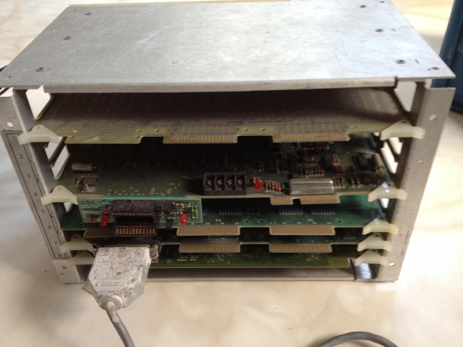
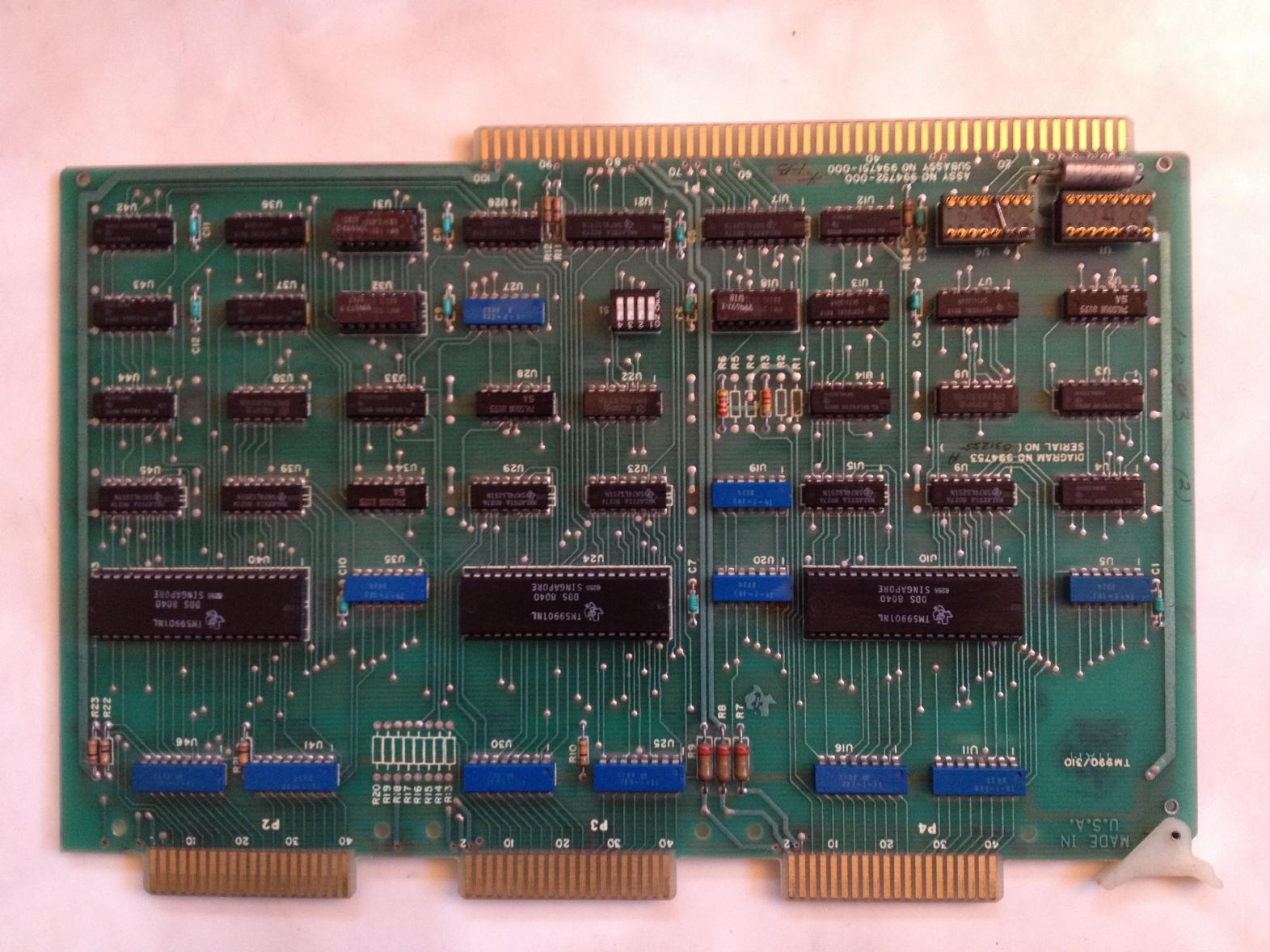
The following pictures show the four boards of the computer (the fifth board which can be seen in the picture above on the right is an empty prototyping board and is thus not shown in the following). From left to right and top to bottom these are the following:
|
|
|

|
|
|
|
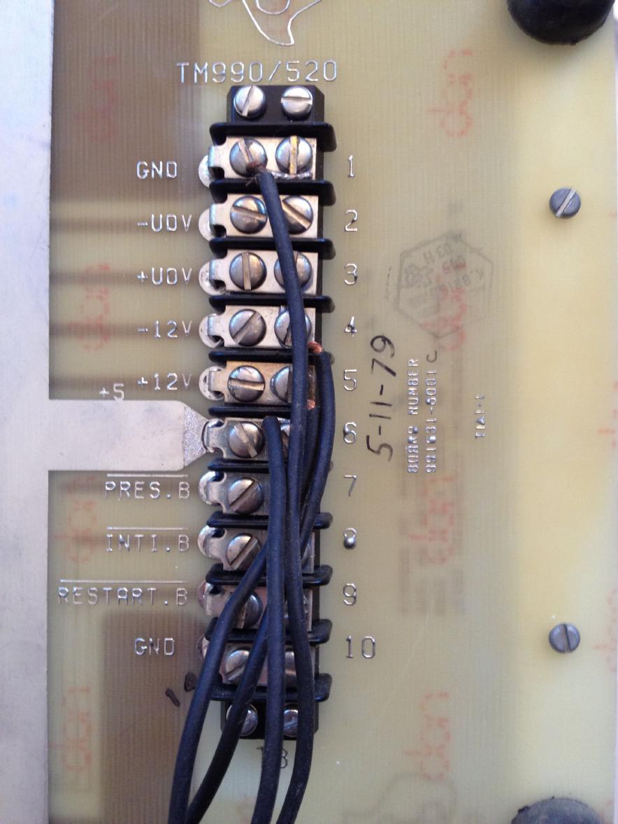
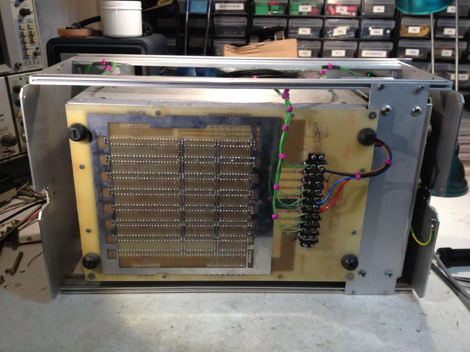
The two following pictures show the 10 slot backplane with its power and signal connector block on the right hand side. The system needs +5 V, +12 V and -12 V (the -5 V required for the TMS9900 CPU chip are derived from the -12 V supply by means of a 7905 linear regulator on the CPU board). In addition to this, there are three interrupt lines which are active-low and can thus be driven by simple push-buttons. |
|

|
|
|
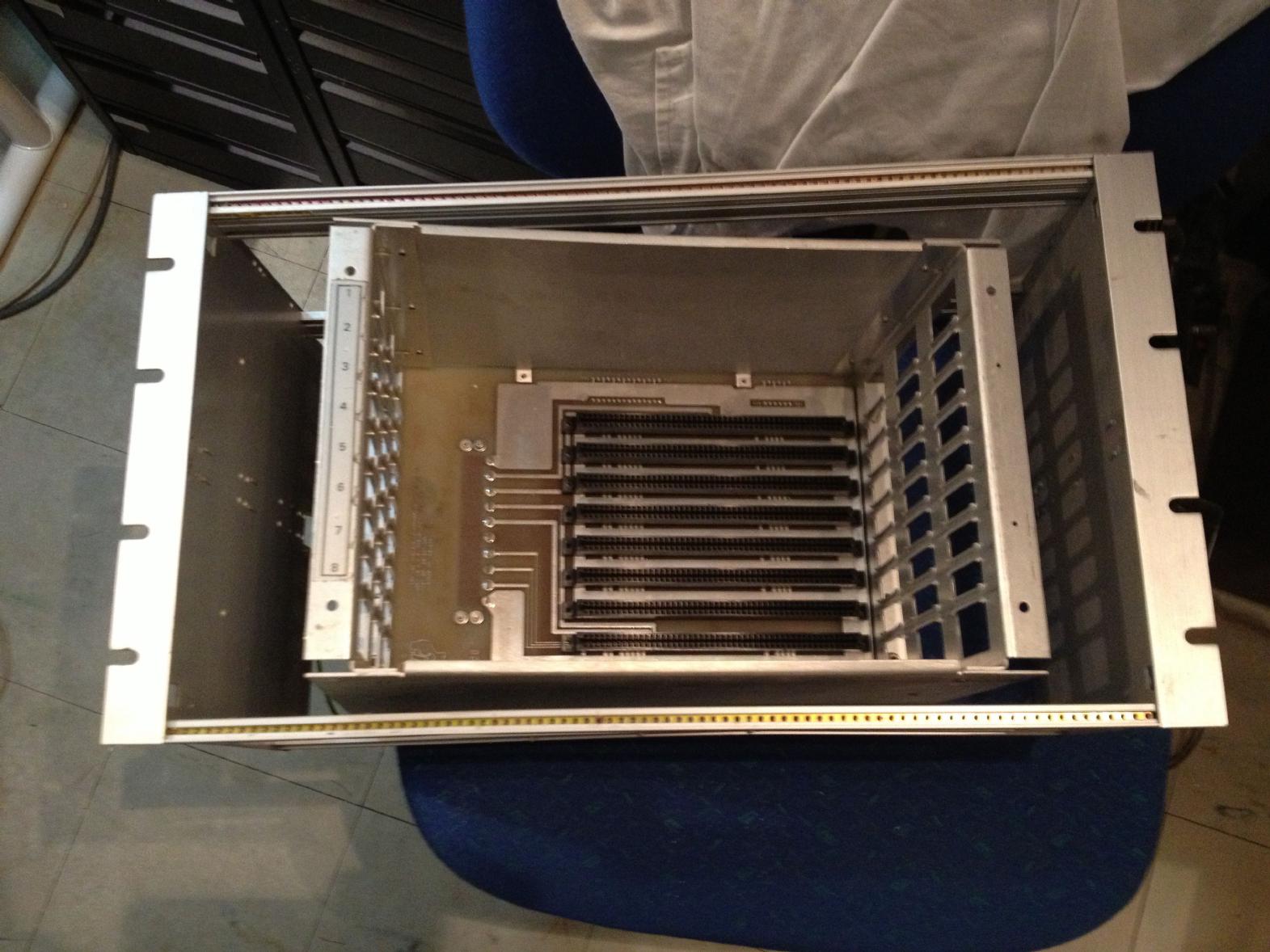
The previous owner ran the system with a linear regulated power supply in this configuration. Somehow I did not like the idea - a computer should at least have a pretty and practical enclosure which would be ideally rack-montable. Fortunately, a couple of months ago I saved a VME-bus crate from a dumpster (I am an avid dumpster diver :-) ) which can be seen in the picture below on the left (it has some scratches and bumps but is basically OK). The picture on the right shows that the TI backplane enclosure fits rather nicely into this larger frame. |
|
|
|
|
|
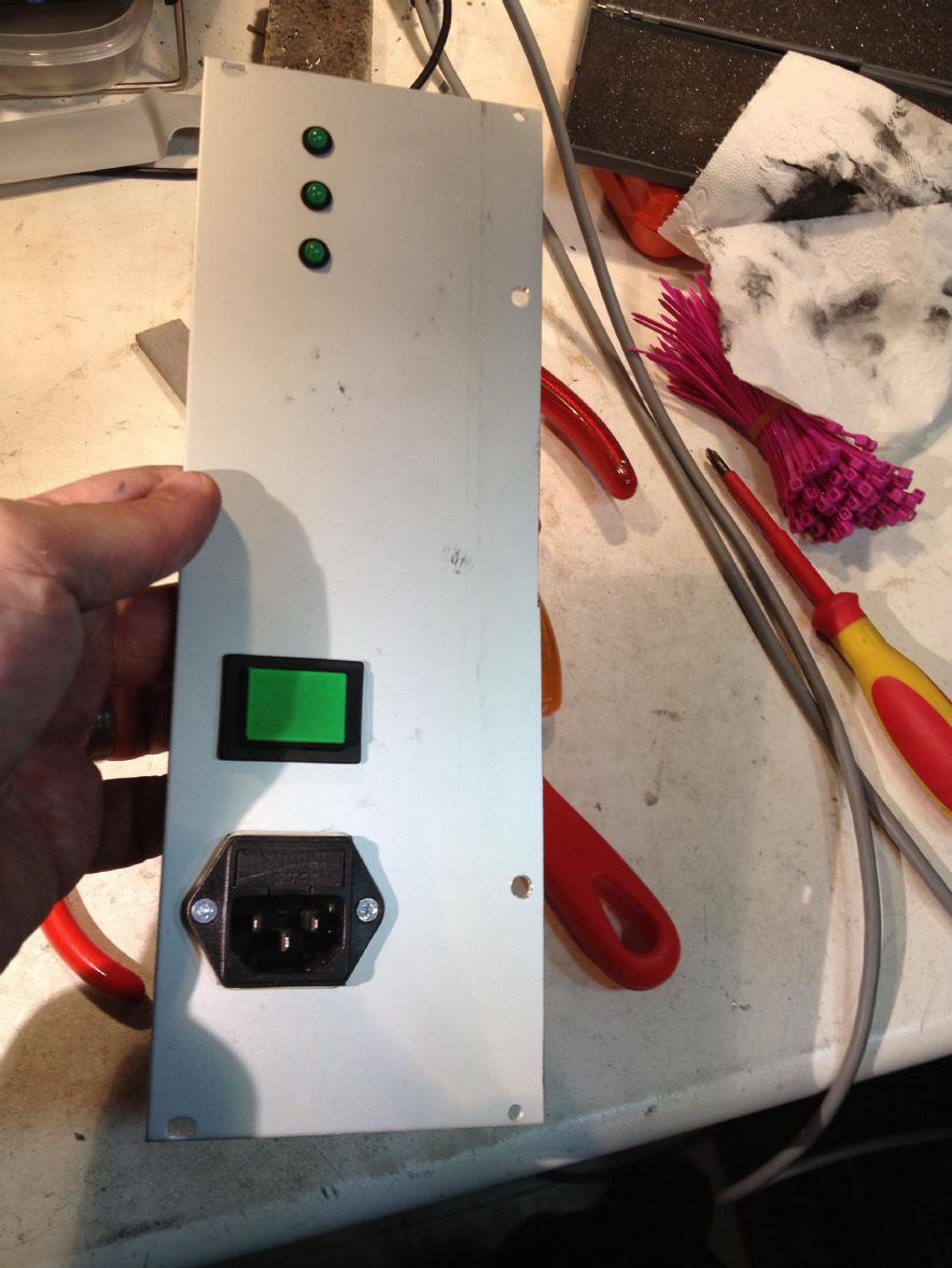
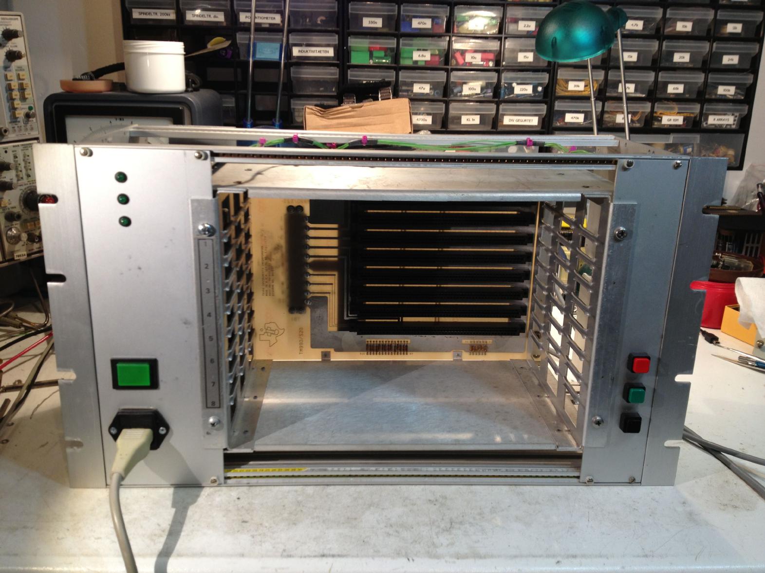
Of course to make everything fit, a little metal working was necessary. The pictures below show the left and right front plate which hold the power connector, power switch, three LEDs to monitor the power supply output lines and the three interrupt switches respectively. |
|
|

|
|
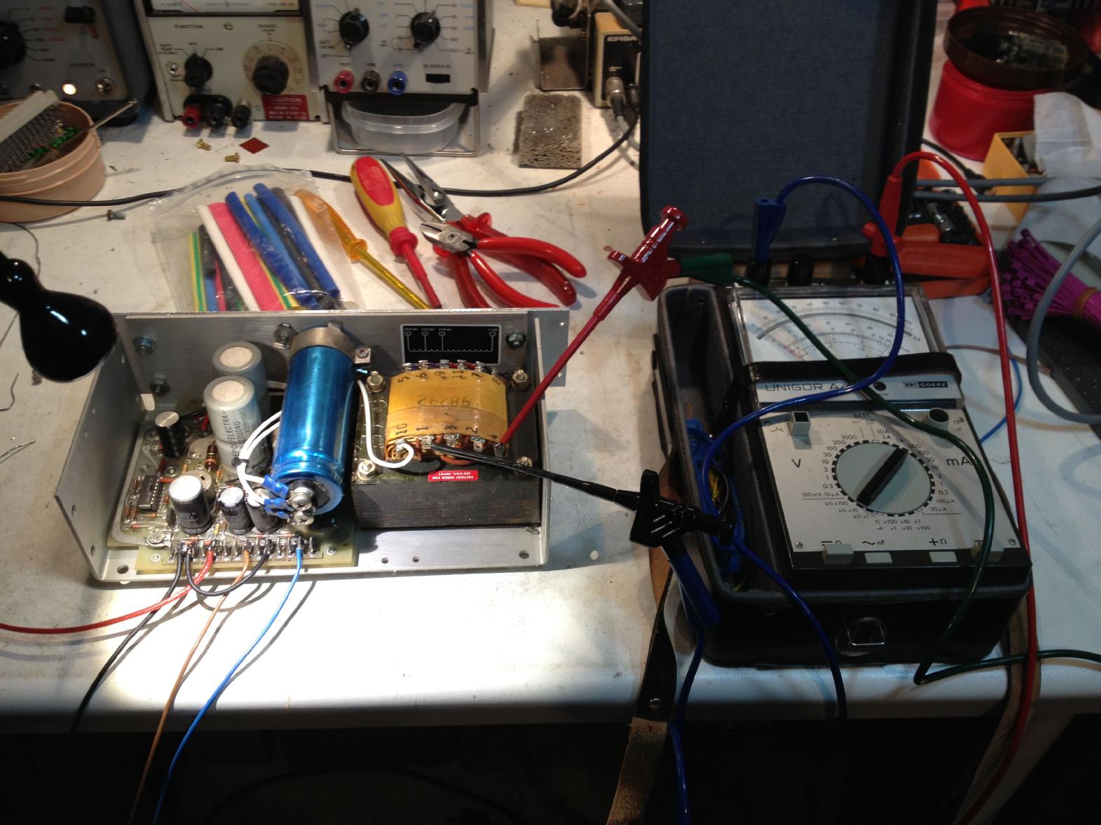
I decided to use the original linearly regulated power supply (it turned out that this was a bad decision - I would have saved some time rebuilding part of the new enclosure if I had directly opted for a modern switched power supply) which can be seen in the picture below on the left. The picture on the right shows this power supply in place, mounted to the left of the backplane assembly. This power supply can deliver 5 V with up to 6 A, which might be a bit tight when running with all of the four boards shown above. |
|
|

|
|
The completed new enclosure can be seen below. The black, brown, blue and red cables running to the connector block from the right are the power supply lines while the thin green wires connect the power supply LEDs and the three interrupt push-buttons. |
|
|
|
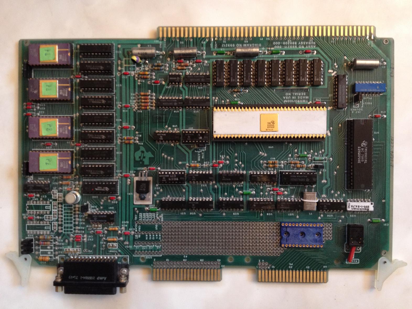
| Repairing the CPU board type 100M: |
|
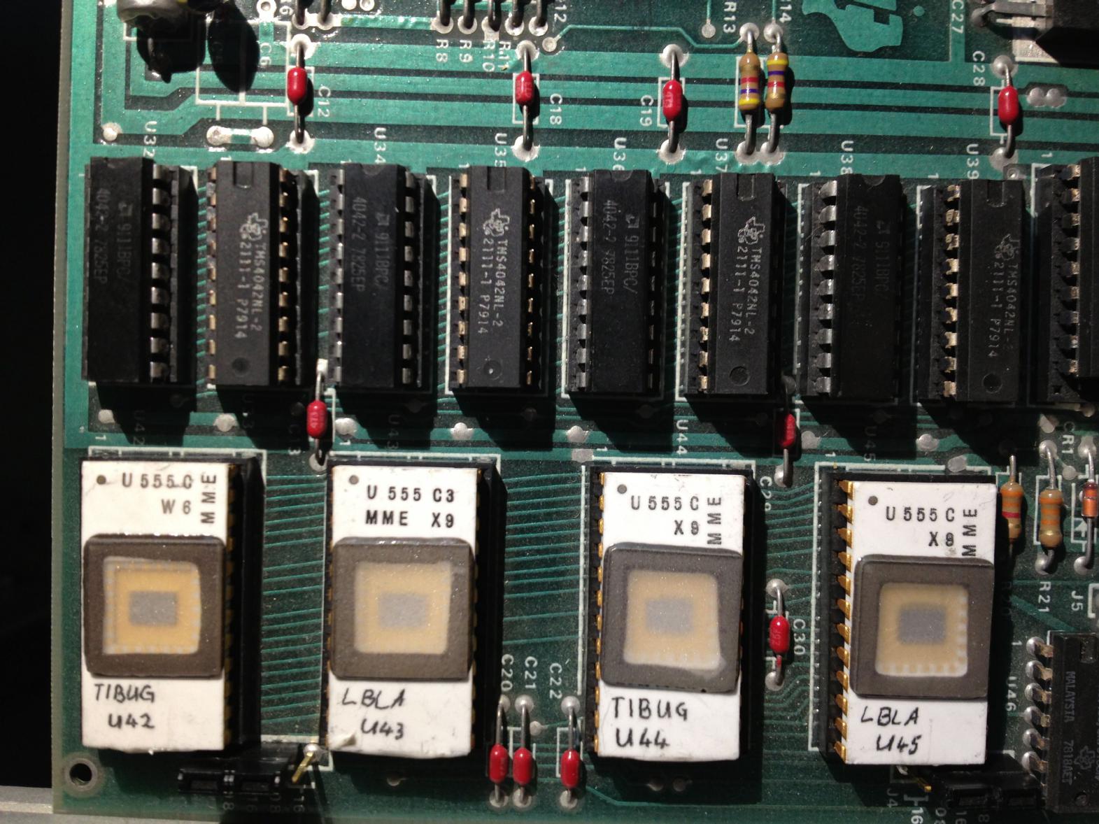
Then the big moment came - first power on. And... ...nothing. Hmmm... Thanks to a partially disassembled listing (thanks, Stuart!) of the BASIC-EPROMs which were originally fitted to the CPU board it became clear that the serial line interface expects the DSR line set to high. Unfortunately there was still no answer from the system after I tied it high with a breakout box. Thanks to a friend, I got the Intel-Hex-images of the extremely simple TIBUG monitor and the line-by-line-assembler (called LBLA :-) ), so I decided to burn a set of four EPROMs to make sure that I have some software which would be simple enough that I could, if necessary, trace the program flow with the help of a logic analyzer and following its progress through a listing. The picture on the right below shows these four "new" EPROMs (2708) containing TIBUG and LBLA. ...and then suddenly, there was a hushed, yet nasty "bzzzt" sound which was the last sign of life from the linear regulator power supply... Somehow the relationship between this computer and me became a bit strained... |
|
|
|
|
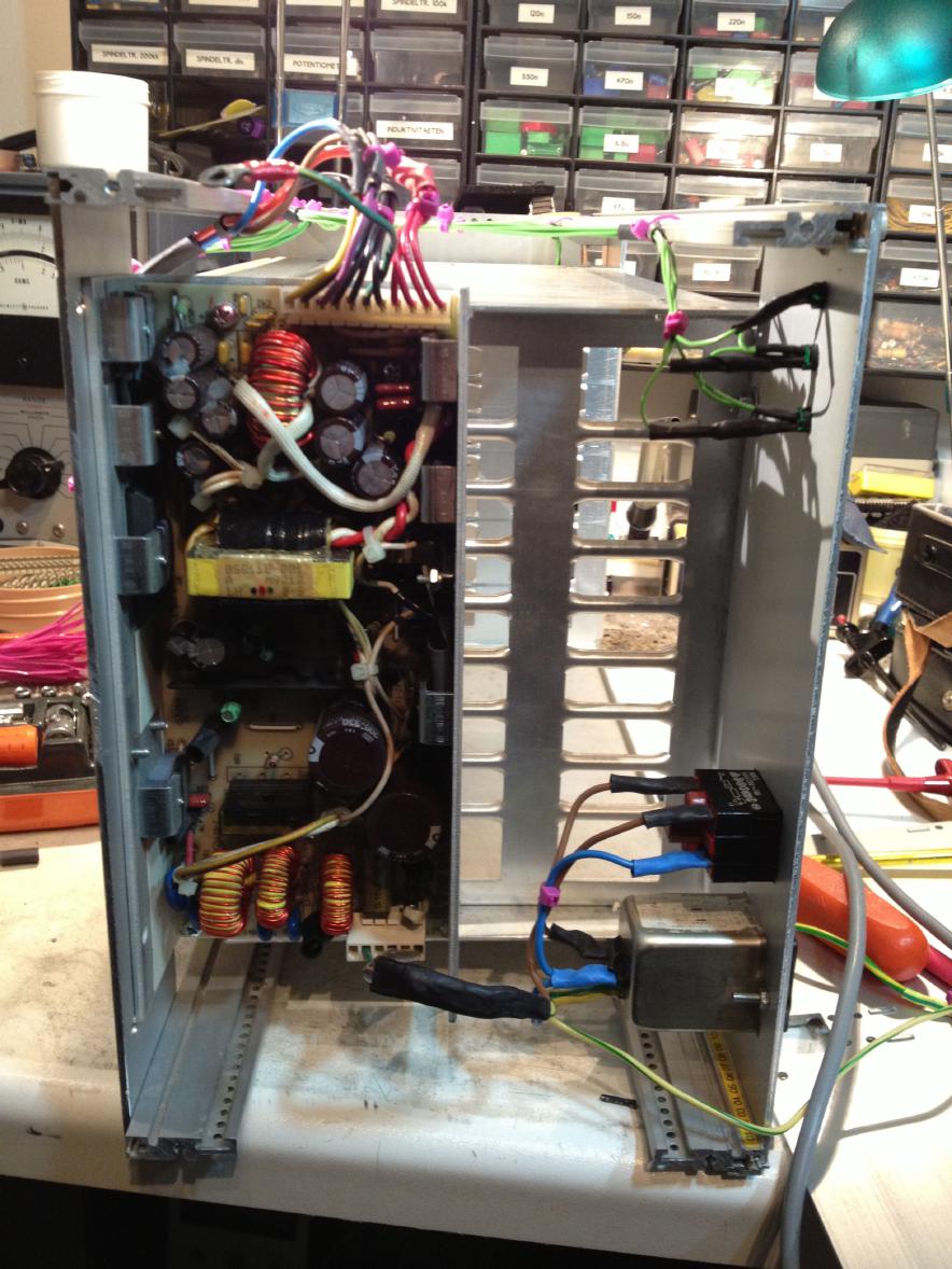
Since the old linear regulator became quite hot even at about 1.5 A at 5 V I decided not to spend time in repairing it (although I did, of course, not throw it away - someday it will be repaired, but not now). Fortunately I had a modern switched power supply in stock (another gem removed from a router found in a dumpster in Frankfurt :-) ), capable of delivering 10 A at 5 V, plenty of power for this system. The picture on the left shows the new power supply in place in the enclosure - I only had to rewire the power supply lines and drill three new holes to mount it to the frame. |
|
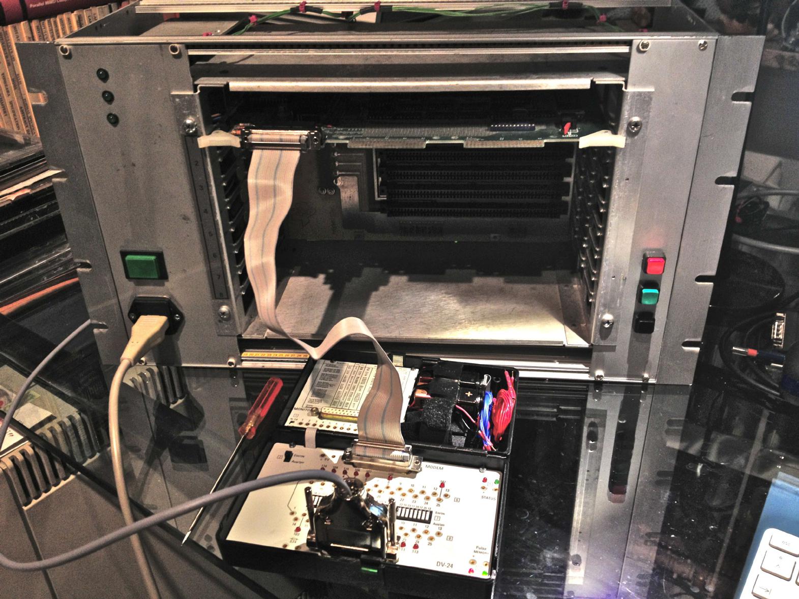
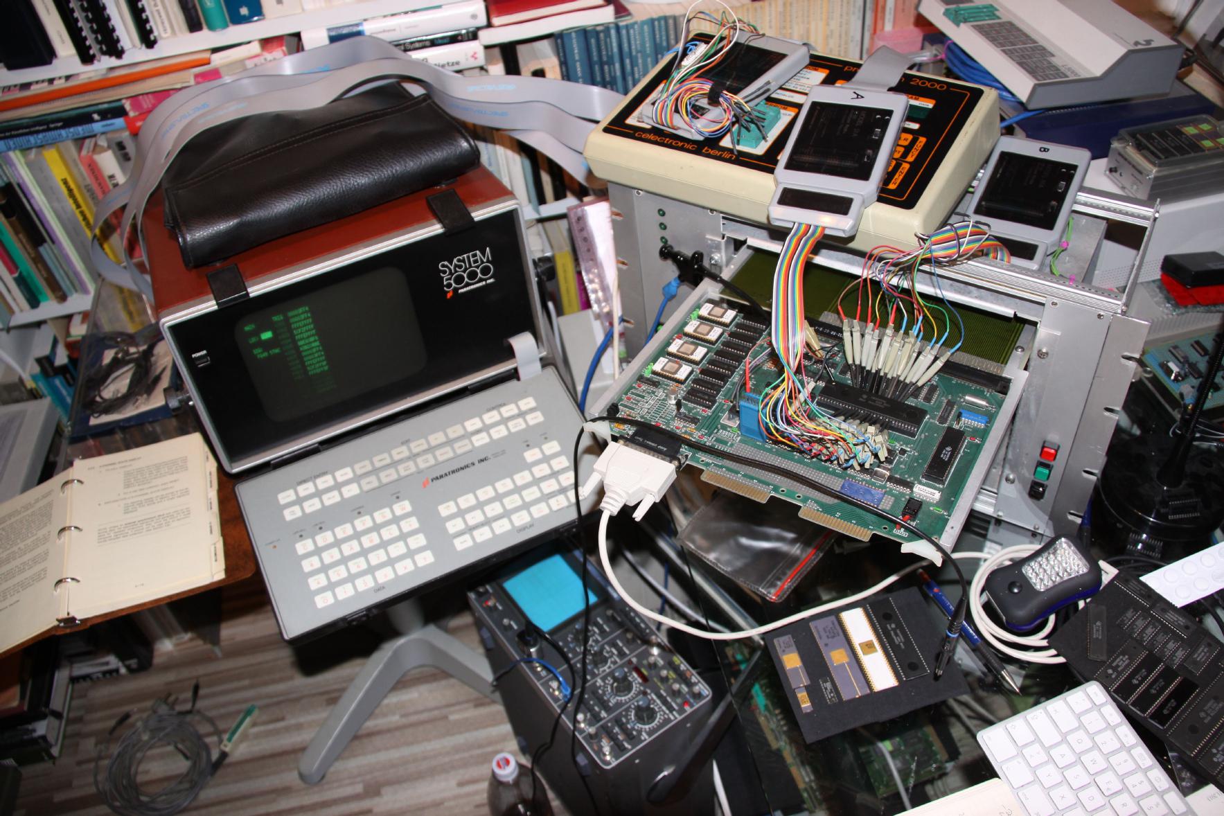
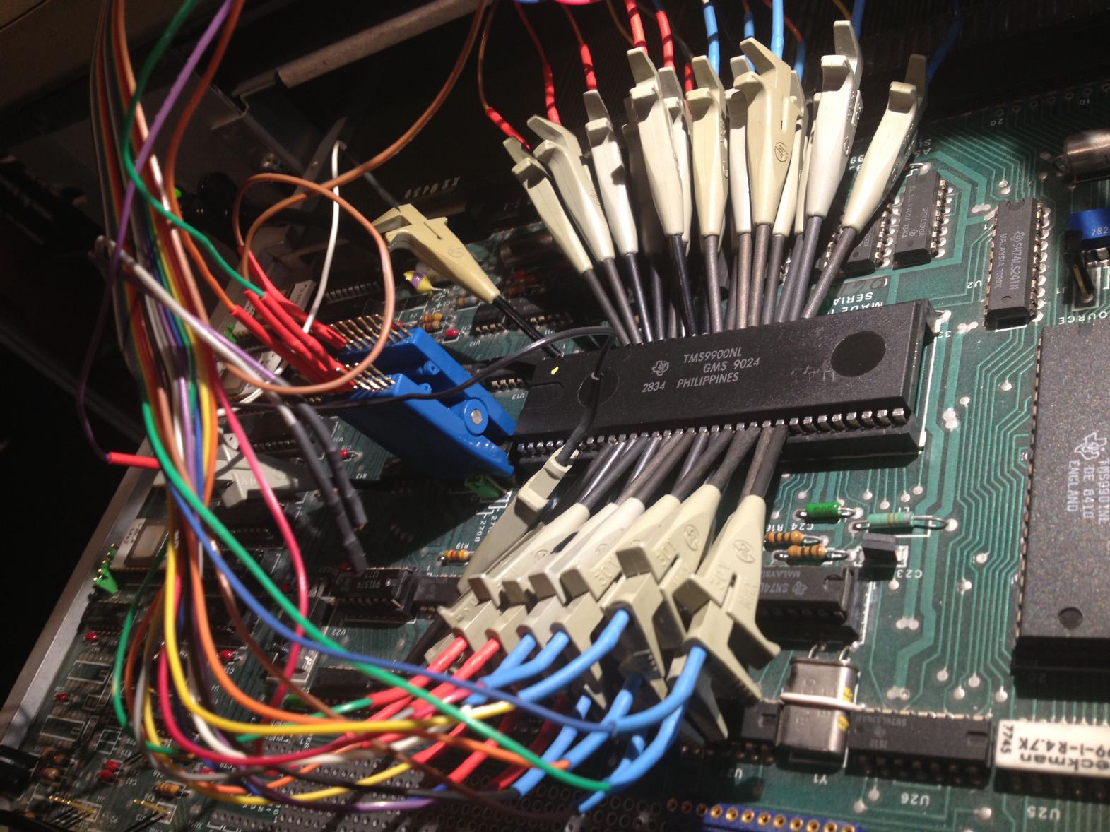
With the new power supply the time had come to start debugging - the picture below on the left shows the overall setup: On the left is my trusty Paratronics SYSTEM 5000 40 channel logic analyzer which I bought in the mid-1990s as a student (even as a used instrument, it cost a fortune - about half what I earned per month, but I never regretted buying it :-) ). On the bottom my dual channel Philips oscilloscope can be seen. On top of the TM990/100M, a promicron 2000 EPROM programmer is visible (this device can program EPROMs down to 2708 which is a rare ability). By the way - if you wonder what happened to the TMS9900 in its white ceramics enclosure, I replaced it by a more recent device just to make sure it would not be harmed during the debugging process. Since I do not have a 64 pin DIP clip, the connections of the logic analyzer to the address and data bus of the TMS9900 and some additional signals of interest look a bit crowded. The clips used are from HP and were sold for their HP1600 line of logic-state analyzers. |
|
|
|
|
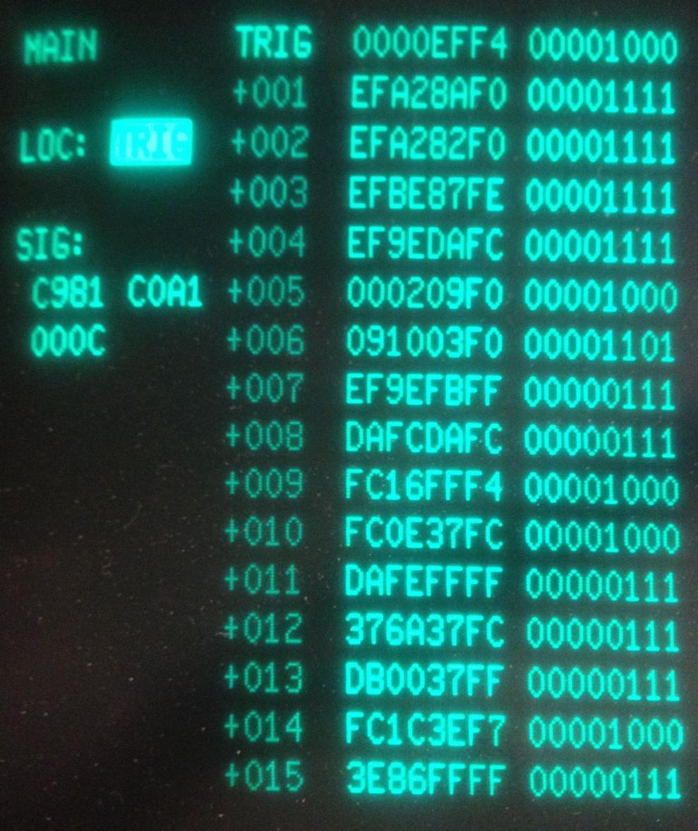
The picture below on the left shows a typical output of the logic analyzer (40 channel state display). The eight hex digits in the second row from the right show the 15 (!) bit address bus (only even addresses) and the corresponding values on the 16 bit data bus. /MEMEN was used as the clock signal for the logic analyzer so I can see everything which is read from or written to memory. The four rightmost bits of the binary display show (from right to left) the control lines /MROM (selects the master ROM containing TIBUG), /EROM (selects the expansion ROM containing LBLA), /RAM (selects RAM) and DBIN (write/read-control). And here it becomes clear that something is definitely wrong with this machine: The three active-low signals for enabling the EPROMs and RAM are always active at the same time! This can be seen quite well in the picture below right. Shown on the oscilloscope are /MROM and /RAM - both are active concurrently which causes the EPROMs and RAMs to drive the data bus lines simultaneously! |
|
|

|
|
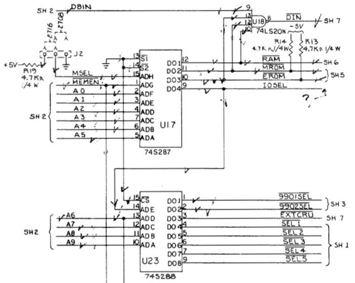
The documentation and schematics reveal that TI uses two PROMs 74S287 and 74S288 for the on-board address decoding which is not good news, since I neither have spare PROMs nor any means of programming such old devices. Since the 74S288 is used only for decoding IO addresses, I concentrated on the 74S287, hoping that only this IC was defective. As one can see in the schematic on the right, there is a total of eight address lines used: MSEL (which switches between 2708 and 2716 EPROMs), /MEMEN (enabling memory access in general) and the six highest address lines from the CPU. |
|
|
With a bit of thought it was simple to reconstruct the contents of this PROM. The fact that TI used an active-high line for IOSEL instead of active-low is brilliant and makes programming a replacement device much easier since a non-programmed (E)PROM location contains a 1. The table below shows the result of my reverse engineering work. Please note that only the lower 4 bits of a data byte of the replacement (E)PROM are used, so the upper nibble is always F. I guess that every address with /MEMEN=1 will activate the IO-address-decoder PROM.
MSEL    /MEMEN  A0  A1  A2  A3  A4  A5! /R  /M  /E  IO  !   ADR !   DATA    !   Comment
--------------------------------------+-----------------+-------+-----------+------------------------
0       0       0   0   0   0   0   0 ! 1   0   1   0   !   00  !   FA      !   Master ROM (2708)
0       0       0   0   0   0   0   1 ! 1   0   1   0   !   01  !   FA      !   Master ROM (2708)
0       0       0   0   0   0   1   0 ! 1   1   0   0   !   02  !   FC      !   Expansion ROM (2708)
0       0       0   0   0   0   1   1 ! 1   1   0   0   !   03  !   FC      !   Expansion ROM (2708)
0       0       1   1   1   1   1   1 ! 0   1   1   0   !   3F  !   F6      !   RAM (1 kB)
--------------------------------------+-----------------+-------+-----------+------------------------
1       0       0   0   0   0   0   0 ! 1   0   1   0   !   80  !   FA      !   Master ROM (2716)
1       0       0   0   0   0   0   1 ! 1   0   1   0   !   81  !   FA      !   Master ROM (2716)
1       0       0   0   0   0   1   0 ! 1   0   1   0   !   82  !   FA      !   Master ROM (2716)
1       0       0   0   0   0   1   1 ! 1   0   1   0   !   83  !   FA      !   Master ROM (2716)
1       0       0   0   0   1   0   0 ! 1   1   0   0   !   84  !   FC      !   Expansion ROM (2716)
1       0       0   0   0   1   0   1 ! 1   1   0   0   !   85  !   FC      !   Expansion ROM (2716)
1       0       0   0   0   1   1   0 ! 1   1   0   0   !   86  !   FC      !   Expansion ROM (2716)
1       0       0   0   0   1   1   1 ! 1   1   0   0   !   87  !   FC      !   Expansion ROM (2716)
1       0       1   1   1   1   1   1 ! 0   1   1   0   !   BF  !   F6      !   RAM (1 kB)
--------------------------------------+-----------------+-------+-----------+------------------------
0       1       X   X   X   X   X   X ! 1   1   1   1   !   40  !   FF      !   IO
                                      !                 !   --  !   FF      !
                                      !                 !   7F  !   FF      !
--------------------------------------+-----------------+-------+-----------+------------------------
1       1       X   X   X   X   X   X ! 1   1   1   1   !   C0  !   FF      !   IO
                                      !                 !   --  !   FF      !
                                      !                 !   FF  !   FF      !
--------------------------------------+-----------------+-------+-----------+------------------------
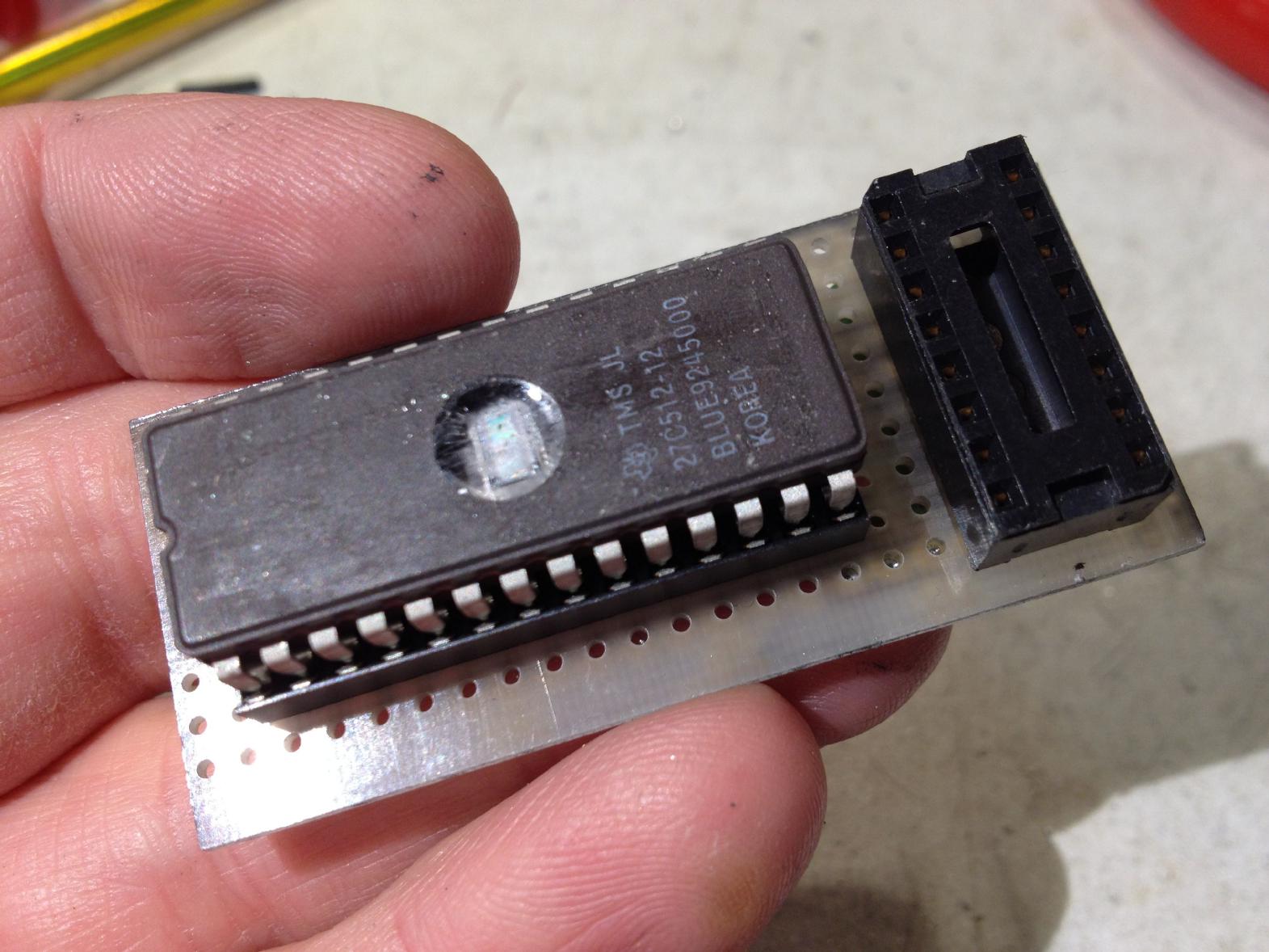
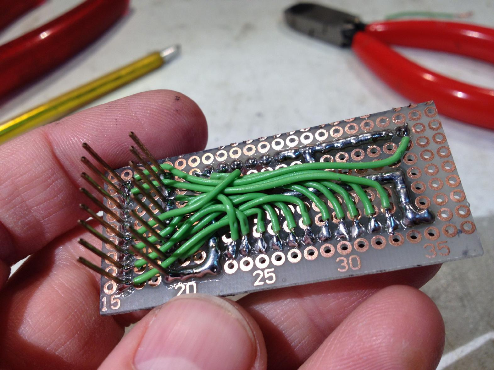
The only problem was now to find a suitable replacement for the 74S287 PROM. This device is quite fast with an access time of 50 ns (in the NL version). An old EPROM like a 2716 etc. was thus ruled out due to its much longer access time. A modern device like a 27C801 would be a good match with 45 ns access time, but I decided to use a 27C512 EPROM (I have quite a lot of those, so nothing to loose) with an access time of 120 ns. The pictures below show my homebrew adapter to fit a 27C512 EPROM to the socket of the original 74S287. The interconnection wiring is as follows (16 pin socket to 28 pin socket):
|
|
|
|
|
The two pictures below show the replacement EPROM in place (left) and an oscilloscope screen-shot showing the active-low select signals /MROM and /RAM. The simultaneous accesses have vanished. |
|

|

|
|
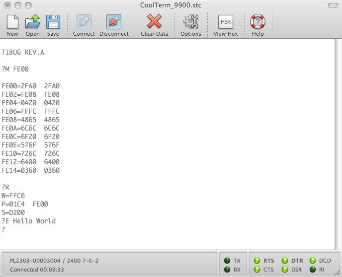
...and, finally, the system is working perfectly! (I am glad that the second PROM, decoding the IO addresses, was not faulty, too.) The picture on the left shows loading and execution of a simple "hello world"-program using the TIBUG monitor. This program was assembled with my simple TMS9900 assembler from this source file:
        .org    $fe00
        xop     text, 14
        blwp    @$fffc
text    .text   "Hello World"
|
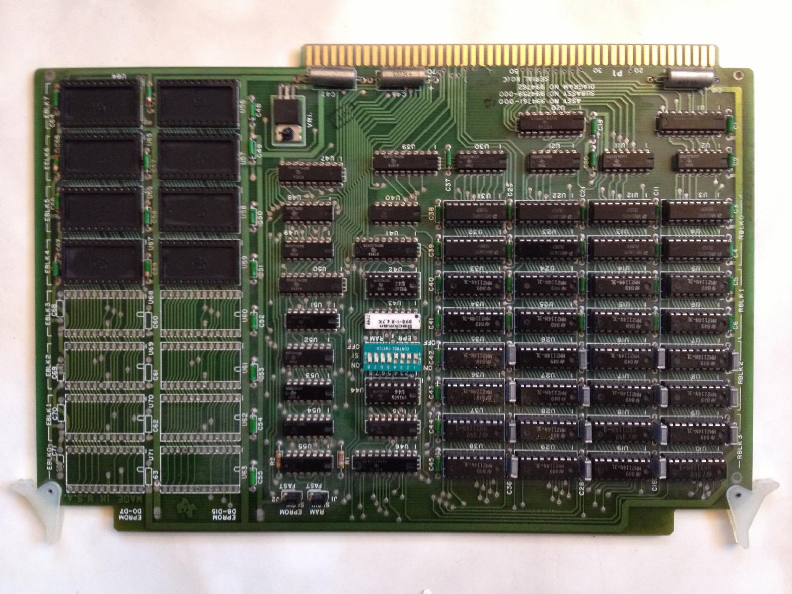
| Repairing the memory board type 201: |
|
Now that the CPU board is working, the next thing I did was inserting the memory board shown above into the backplane. Guess what... It does not work. This machine does its best to teach me some lessons on debugging TI circuitry. After I discovered that at least some and not all memory cells are at fault (so there is no problem in the bus drivers and associated circuitry), I wrote the following small test program to write bit patterns to memory, read them back and print a list of faults memory cells. The output of the assembler looks like this (just in case anybody needs a simple memory exerciser and has no assembler at hand):
                                     .org  $fc00
                    no_of_pattern    .equ  $8
FC00 0201 0008                       li    r1, no_of_pattern   ; Number of patterns
FC04 0203 EFFE                       li    r3, $effe           ; End address
FC08 0641           p_loop           dect  r1                  ; Process next pattern
FC0A C021 FC3A                       mov   @pattern(r1), r0    ; Load pattern
FC0E 2FA0 FC42                       xop   @p_text, 14
FC12 2E80                            xop   r0, 10              ; Print pattern
FC14 2FA0 FC52                       xop   f_text, 14
FC18 0202 B000                       li    r2, $b000           ; Start address
FC1C 80C2           loop             c     r2, r3              ; End reached?
FC1E 1309                            jeq   next                ; Yes
FC20 C480                            mov   r0, *r2             ; Write pattern to memory
FC22 C112                            mov   *r2, r4             ; Read the pattern back
FC24 8004                            c     r4, r0              ; Compare patterns
FC26 1303                            jeq   l_1                 ; OK, write next memory cell
FC28 2E82                            xop   r2, 10
FC2A 2FA0 FC68                       xop   @blank, 14
FC2E 05C2           l_1              inct  r2
FC30 10F5                            jmp   loop                ; Write next word
FC32 C000           next             mov   r0, r0              ; End reached?
FC34 16E9                            jne   p_loop              ; Start writing next pattern
FC36 0420 FFFC      exit             blwp  @$fffc              ; Return to monitor
FC3A 0000 5555 AAAA
     FFFF           pattern          .data $0000, $5555, $aaaa, $ffff
FC42 0D0A 5445 5354
     5041 5454 4552
     4E3A 2000      p_text           .text "\nTESTPATTERN: "
FC52 0D0A 4641 554C
     5459 2041 4444
     5245 5353 4553
     3A20 0000      f_text           .text "\nFAULTY ADDRESSES: "
FC68 2000           blank            .text " "
The results of running this program on my TM990/100M are a bit discouraging (this is just the output for one of the four test bit patterns):
FAULTY ADDRESSES: B000 B002 B004 B006 B008 B00A B00C B00E B010 B012 B014 B016
B018 B01A B01C B01E B020 B022 B024 B026 B028 B02A B02C B02E B030 B032 B034 B036
B038 B03A B03C B03E B040 B042 B044 B046 B048 B04A B04C B04E B050 B052 B054 B056
B058 B05A B05C B05E B060 B062 B064 B066 B068 B06A B06C B06E B070 B072 B074 B076
B078 B07A B07C B07E B080 B082 B084 B086 B088 B08A B08C B08E B090 B092 B094 B096
B098 B09A B09C B09E B0A0 B0A2 B0A4 B0A6 B0A8 B0AA B0AC B0AE B0B0 B0B2 B0B4 B0B6
B0B8 B0BA B0BC B0BE B0C0 B0C2 B0C4 B0C6 B0C8 B0CA B0CC B0CE B0D0 B0D2 B0D4 B0D6
B0D8 B0DA B0DC B0DE B0E0 B0E2 B0E4 B0E6 B0E8 B0EA B0EC B0EE B0F0 B0F2 B0F4 B0F6
B0F8 B0FA B0FC B0FE B1E0 B1E2 B1E4 B1E6 B1E8 B1EA B1EC B1EE B1F0 B1F2 B1F4 B1F6
B1F8 B1FA B1FC B1FE B200 B202 B204 B206 B208 B20A B20C B20E B210 B212 B214 B216
B218 B21A B21C B21E B220 B222 B224 B226 B228 B22A B22C B22E B230 B232 B234 B236
B238 B23A B23C B23E B240 B242 B244 B246 B248 B24A B24C B24E B250 B252 B254 B256
B258 B25A B25C B25E B260 B262 B264 B266 B268 B26A B26C B26E B270 B272 B274 B276
B278 B27A B27C B27E B280 B282 B284 B286 B288 B28A B28C B28E B290 B292 B294 B296
B298 B29A B29C B29E B2A0 B2A2 B2A4 B2A6 B2A8 B2AA B2AC B2AE B2B0 B2B2 B2B4 B2B6
B2B8 B2BA B2BC B2BE B2C0 B2C2 B2C4 B2C6 B2C8 B2CA B2CC B2CE B2D0 B2D2 B2D4 B2D6
B2D8 B2DA B2DC B2DE B2E0 B2E2 B2E4 B2E6 B2E8 B2EA B2EC B2EE B2F0 B2F2 B2F4 B2F6
B2F8 B2FA B2FC B2FE B3E0 B3E2 B3E4 B3E6 B3E8 B3EA B3EC B3EE B3F0 B3F2 B3F4 B3F6
B3F8 B3FA B3FC B3FE B400 B402 B404 B406 B408 B40A B40C B40E B410 B412 B414 B416
B418 B41A B41C B41E B420 B422 B424 B426 B428 B42A B42C B42E B430 B432 B434 B436
B438 B43A B43C B43E B440 B442 B444 B446 B448 B44A B44C B44E B450 B452 B454 B456
B458 B45A B45C B45E B460 B462 B464 B466 B468 B46A B46C B46E B470 B472 B474 B476
B478 B47A B47C B47E B480 B482 B484 B486 B488 B48A B48C B48E B490 B492 B494 B496
B498 B49A B49C B49E B4A0 B4A2 B4A4 B4A6 B4A8 B4AA B4AC B4AE B4B0 B4B2 B4B4 B4B6
B4B8 B4BA B4BC B4BE B4C0 B4C2 B4C4 B4C6 B4C8 B4CA B4CC B4CE B4D0 B4D2 B4D4 B4D6
B4D8 B4DA B4DC B4DE B4E0 B4E2 B4E4 B4E6 B4E8 B4EA B4EC B4EE B4F0 B4F2 B4F4 B4F6
B4F8 B4FA B4FC B4FE B5E6 B5EC B5F4 B5F8 B5FA B5FC B600 B602 B604 B606 B608 B60A
B60C B60E B610 B612 B614 B616 B618 B61A B61C B61E B620 B622 B624 B626 B628 B62A
B62C B62E B630 B632 B634 B636 B638 B63A B63C B63E B640 B642 B644 B646 B648 B64A
B64C B64E B650 B652 B654 B656 B658 B65A B65C B65E B660 B662 B664 B666 B668 B66A
B66C B66E B670 B672 B674 B676 B678 B67A B67C B67E B680 B682 B684 B686 B688 B68A
B68C B68E B690 B692 B694 B696 B698 B69A B69C B69E B6A0 B6A2 B6A4 B6A6 B6A8 B6AA
B6AC B6AE B6B0 B6B2 B6B4 B6B6 B6B8 B6BA B6BC B6BE B6C0 B6C2 B6C4 B6C6 B6C8 B6CA
B6CC B6CE B6D0 B6D2 B6D4 B6D6 B6D8 B6DA B6DC B6DE B6E0 B6E2 B6E4 B6E6 B6E8 B6EA
B6EC B6EE B6F0 B6F2 B6F4 B6F6 B6F8 B6FA B6FC B6FE
Interestingly, all of these faults were caused by a single 2114 RAM chip. Fortunately, I had a spare part. Replacing this IC fixed the memory problem.
|
|
| Repairing the software development board type 302: |
|
Now that I have a working CPU and memory expansion board, I would love to run "Development-BASIC" on this machine. This interpreter comes in six or eight (if the "Enhancement" package is installed) EPROMs 2716, four of which mount on the 100M CPU board and two/four normally mount on the type 302 "software development board". Normally, the lower 8 kB EPROM reside on the CPU in address space $0000 to $1FFE (remember, there are only 15 address bits with the LSB being implicitly set to zero) while the upper 8 kB (assuming that the "Enhancement" package is installed, too) reside on the 302 board and map into the address space $2000 to $3FFE. Poking around in memory a bit with the help of TIBUG, it turned out that the 302 board is invisble. Nothing... No access to the EPROMs on the board - and I had already hoped that I could put the logic analyzer back into the closet... It is next to unbelievable - it looks as if the address decoding PROM on the 302 board is defective, too. Its outputs are always inactive, thus neither on-board ROM nor RAM are activated. Time to build yet another small adapter board for an address decoding EPROM, but not today, I think. |