| |
|
A high performance amplifier for seismic applications
|
|---|
|
After building a passive seismometer of the Lehman type or something like that, the next problem is the amplification of the tiny signals obtained by an instrument like this. So the first attribute to ask for in an amplifier for seismic application is a large gain in the range of about 10000. The next necessary attribute is a low pass filter to get rid of
These necessary attributes lead to the following design: The amplifier consists of five major building blocks:
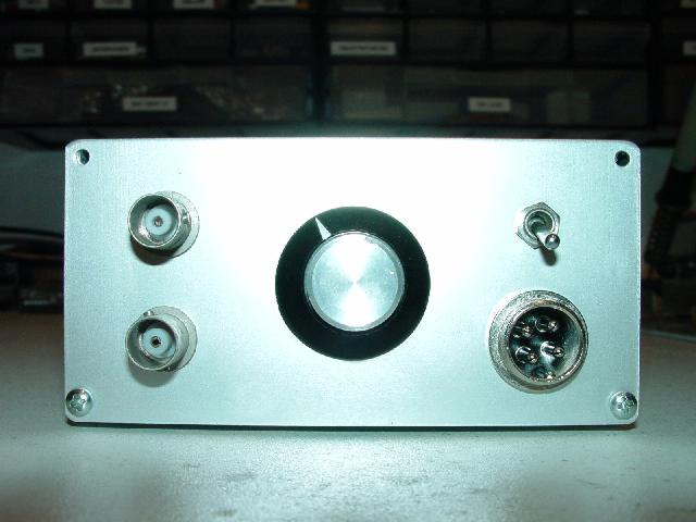
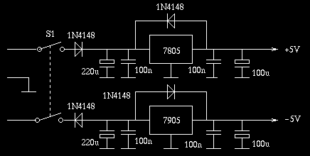
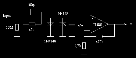
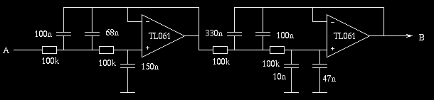
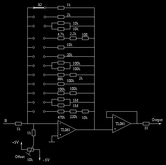
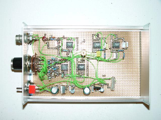
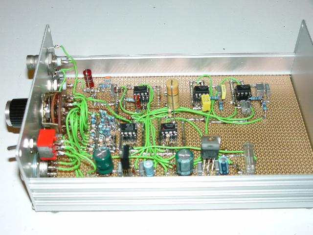
The schematic of the first building block, the power supply is shown below. It is really a very simple power supply requiring a symmetric input voltage of +/-7 to +/- 30 volts which is stabilized (after passing an electrolytic capacitor) by a pair of 7805/7905 stabilizer circuits (which are protected by diodes in case of a back current occurring after a power off). The next stage is the input amplifier with its associated circuitry as shown in the following picture: The input section consists of a 10M resistor to ground, followed by an R/C-circuit which is itself followed by a pair of antiparallel protection diodes to assure that the input of the following operating amplifier will not receive more than about 0.7 Volts. The 68n capacitor is necessary to avoid oscillatory behaviour of the amplifier circuit. The amplifier itself is used in a non inverting configuration so its input resistance is very high (so the resistance of the whole input section as seen by external equipment is determined mainly by the passive input circuitry). The amplifier is wired to have a gain of 100. The next section is the four pole Butterworth low pass filter with its cut off frequency of 10 Hz: Following the Butterworth filter is the main amplifier with its resistor controlled, selectable gain ranging from 1 to 700. This amplifier and the following impedance converter is shown in the next picture. Note the offset potentiometer at the lower left side of the drawing. This is necessary to compensate for offsets introduced by the preceeding stages which would lead to an overdriven main amplifier (at least in its highed gain setting) and thus in a loss of the signal of interest. The next picture shows the interior of the completed prototype amplifier. On the lower part of the circuit board, the power supply circuitry can be seen. In the upper left part, the input section with its passive network and the first stage amplifier may be seen. This amplifier is followed by the Butterworth low pass filter located in the upper right part of the amplifier. In the left middle part, the resistive gain control network can be seen in conjunction with the main amplifier which is itself followed directly by the impedance converter. The next and last picture shows the interior again but from a different angle: |